Technological process 28 nm. What is the processor technology process and what does it affect? What does the technical process affect?
Despite the fact that the technical process does not directly affect the performance of the processor, we will still mention it as a characteristic of the processor, since it is the technical process that influences the increase in processor performance through design changes. I would like to note that the technical process is a general concept for both central processors and graphics processors that are used in video cards.
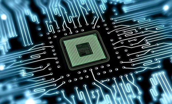
The main element in processors are transistors - millions and billions of transistors. The principle of operation of the processor follows from this. A transistor can both pass and block electric current, which allows logic circuits to operate in two states - on and off, that is, in the well-known binary system (0 and 1).
The process technology is essentially the size of the transistors. And the basis of processor performance lies precisely in transistors. Accordingly, the smaller the transistors, the more of them can be placed on the processor chip.
New Intel processors are made using the 22 nm process technology. A nanometer (nm) is 10 to the -9 power of a meter, which is one billionth of a meter. So that you can better imagine how miniature these transistors are, I’ll give you one interesting scientific fact: “With the help of modern technology, 2000 transistor gates can be placed on the cross-sectional area of a human hair!”
If we take into account modern processors, then the number of transistors there has long exceeded 1 billion.
Well, the technical process of the first models did not begin with nanometers at all, but with larger volumetric quantities, but we will not return to the past.
Examples of technical processes of graphical and central processing units
Now we will look at a couple of the latest technical processes used by well-known manufacturers of graphics and central processors.
1. AMD (processors):
Technological process 32 nm. These include Trinity, Bulldozer, Llano. For example, in Bulldozer processors, the number of transistors is 1.2 billion, with a crystal area of 315 mm2.
Technological process 45 nm. These include Phenom and Athlon processors. An example here would be Phemom, with a number of transistors of 904 million and a crystal area of 346 mm2.
2.Intel:
Technological process 22 nm. Ivy Bridge processors (Intel Core ix - 3xxx) are built according to 22 nm standards. For example, Core i7 – 3770K, has 1.4 billion transistors on board, with a crystal area of 160 mm2, we see a significant increase in placement density.

Technological process 32 nm. These include Intel Sandy Bridge processors (Intel Core ix – 2xxx). Here, 1.16 billion are located on an area of 216 mm2.
Here you can clearly see that according to this indicator, Intel is clearly ahead of its main competitor.
3. AMD (ATI) (video cards):
Technological process 28 nm. Radeon HD 7970 video card
4. Nvidia:
Technological process 28 nm. GeForce GTX 690

So we looked at the concept of technical process in central and graphic processors. Today, developers plan to conquer the 14 nm process technology, and then 9, using other materials and methods. And this is far from the limit!
we-it.net
What is the processor technology process and what does it affect?
All modern computing technologies are based on semiconductor electronics. For its production, silicon crystals are used - one of the most common minerals in our planet. Since the demise of bulky tube systems and the development of transistor technology, this material has occupied an important place in the production of computer equipment.
Central and graphic processors, memory chips, various controllers - all this is produced on the basis of silicon crystals. For half a century, the basic principle has not changed, only chip creation technologies are being improved. They are becoming thinner and more miniature, energy efficient and productive. The main parameter that will be improved is the technical process.
What is a technical process
Almost all modern chips consist of silicon crystals, which are processed by lithography to form individual transistors. The transistor is the key element of any integrated circuit. Depending on the state of the electric field, it can transmit a value equivalent to a logical one (passes current) or zero (acts as an insulator). In memory chips, data is written using combinations of zeros and ones (transistor positions), and in processors, calculations are performed when switching.

In 14-nm technology (compared to 22-nm), the number of barriers is reduced, their height is increased, and the distance between the dielectric fins is reduced
A technological process is a procedure and procedure for manufacturing any product. In the electronics industry, in its generally accepted meaning, this is a value that indicates the resolution of the equipment used in the production of chips. The size of the functional elements obtained after silicon processing (that is, transistors) also directly depends on it. The more sensitive and accurate the equipment used for processing crystals for processor blanks, the finer the technical process will be.
What does the numerical value of a technical process mean?
In modern semiconductor manufacturing, the most common method is photolithography - etching elements on a chip coated with a dielectric film using light. It is the resolution of the optical equipment that emits light for etching that is the technical process in the generally accepted interpretation of the word. This number indicates how thin the feature on the chip can be.

Photolithography - etching elements on a crystal
What does the technical process affect?
The technical process directly affects the number of active elements of a semiconductor chip. The thinner the technical process, the more transistors will fit on a certain area of the chip. First of all, this means increasing the number of products from one piece. Secondly, reducing energy consumption: the thinner the transistor, the less energy it consumes. As a result, with an equal number and arrangement of transistors (and therefore an increase in performance), the processor will consume less energy.
The downside of switching to a fine technical process is that the equipment will become more expensive. New industrial units make it possible to make processors better and cheaper, but they themselves increase in price. As a result, only large corporations can invest billions of dollars in new equipment. Even such well-known companies as AMD, Nvidia, Mediatek, Qualcomm or Apple do not make processors themselves, entrusting this task to giants like TSMC.
What does reducing the technical process give?
By reducing the technological process, the manufacturer has the opportunity to increase performance while maintaining the same chip dimensions. For example, the transition from 32 nm to 22 nm made it possible to double the transistor density. As a result, on the same chip as before, it became possible to place not 4, but already 8 processor cores.
For users, the main benefit is reduced energy consumption. Chips using a thinner process technology require less energy and generate less heat. Thanks to this, you can simplify the power system, reduce the cooler, and pay less attention to blowing components.

Schematic forecast of process changes in the future
Processor technology on smartphones
Smartphones are demanding on hardware resources and quickly drain battery power. Therefore, to slow down the discharge consumption, developers of processors for mobile devices are trying to introduce the latest technical processes into production. For example, the once popular dual-core MediaTek MT6577 was produced using a 40 nm process technology, and Qualcomm Snapdragon 200 early series were manufactured using 45 nm technology.
In 2013-2015, 28 nm became the main technological process for chips used in smartphones. MediaTek (up to and including Helio X10), Qualcomm Snapdragon S4, 400 series, as well as models 600, 602, 610, 615, 616 and 617 are all 28 nm. It was also used in the manufacture of Snapdragon 650, 652, 800, 801, 805. The “hot” Snapdragon 810, interestingly, was made using a thinner 20 nm process technology, but this did not help it much.
Apple also used 20nm technology in its A7 (iPhone 5S). The Apple A8 for the sixth iPhone used 20 nm, and the A9 model (for 6s and SE) already uses the new 16 nm process technology. In 2013-2014, Intel made their Atom Z3xxx using 22-nanometer technology. Since 2015, chips with 14 nm have been launched into production.
The next step in the development of processors for smartphones is the widespread development of 14 and 16 nm technological processes, and then we can expect 10 nm. The first copies on it may be Qualcomm Snapdragon 825, 828 and 830.
mobcompany.info
What is the technical process in a processor: the importance of crystal size
09.07.2017  Blog of Dmitry Vassiyarov.
Good day.
Let's together lift the veil of such a complex matter as the production of CPUs for computers. In particular, from this article you will learn what the technical process in a processor is and why every year developers are trying to reduce it.
How are processors made?
First, you should know the answer to this question so that further explanations are clear. Any electronic equipment, including the CPU, is created on the basis of one of the most commonly used minerals - silicon crystals. Moreover, it has been used for these purposes for more than 50 years.
The crystals are processed through lithography to enable the creation of individual transistors. The latter are the fundamental elements of the chip, since it consists entirely of them.

The function of transistors is to block or pass current, depending on the current state of the electric field. Thus, logic circuits operate in a binary system, that is, in two positions - on and off. This means that they either transmit energy (logical one) or act as insulators (zero). When switching transistors in the CPU, calculations are performed.
Now about the main thing
Generally speaking, the technological process refers to the size of the transistors.
What does it mean? Let's return to the production of processors again.
The most commonly used method is photolithography: the crystal is covered with a dielectric film, and transistors are etched from it using light. For this purpose, optical equipment is used, the resolution of which, in essence, is a technical process. The thinness of the transistors on the crystal depends on its value - on the accuracy and sensitivity of the device.

What does this give?
As you understand, the smaller they are, the more of them can be placed on the chip. This affects:
- Heat dissipation and power consumption. By reducing the size of the element, it requires less energy and therefore generates less heat. This advantage allows you to install powerful CPUs in small mobile devices. By the way, thanks to the low power consumption of modern chips, tablets and smartphones hold their charge longer. For PCs, lower heat dissipation makes it possible to simplify the cooling system.
- Number of blanks. On the one hand, it is beneficial for manufacturers to reduce the technical process, because a larger quantity of products is obtained from one workpiece. True, this is only a consequence of the refinement of the technical process, and not the pursuit of benefits, because on the other hand, to reduce the size of transistors, more expensive equipment is needed.

- Chip performance. The more elements it has, the faster it will work, while its physical size will remain the same.
Technological process in numbers and examples
The technological process is measured in nanometers (nm). This is 10 to the -9 power of a meter, that is, one nanometer is a billionth of it. On average, modern processors are manufactured using a 22 nm process technology.
You can imagine how many transistors fit on a processor. To make it clearer, the cut area of a human hair can accommodate 2,000 elements. Although the chip is miniature, it is clearly larger than a hair, so it can include billions of transistor gates.
Want to know more precisely? Let me give you a few examples:
- AMD processors, namely Trinity, Llano, Bulldozer, have a 32 nm process technology. In particular, the crystal area of the latter is 315 mm2, where 1.2 billion transistors are located. Phenom and Athlon from the same manufacturer are made using a 45 nm process technology, that is, they have 904 million with a base area of 346 mm2.

- Intel has chips based on the 22 nm standard - this is the Ivy Bridge family (Intel Core ix - 3xxx). For clarity: Core i7 – 3770K has 1.4 billion elements, despite the fact that its die size is only 160 mm. The same brand also has 32nm products. We are talking about Intel Sandy Bridge (2xxx). On an area of 216 mm2 it fits 1.16 billion transistors.

By the way, everything you learned about technical processes for central computer devices also applies to graphics devices. For example, this value in AMD (ATI) and Nvidia video cards is 28 nm.

Now you know more about such an important component of your computer as the processor. Come back for more information.
See you later.
Intel: Our 10nm process will be the best in the industry
Intel has confirmed a delay in mass production of CPUs using the 10nm process until the second half of 2017. The chipmaker claims that due to difficulties in mastering new production standards, it will have to extend the life cycle of the 14nm CPU process by another year. Thus, next year Intel will introduce Kaby Lake processors, and Cannonlake will be released only in 2017. Intel management admitted that due to the increasing complexity of chip production, the famous Moore's law may undergo transformation. However, unlike competitors, Intel has no plans to simplify the characteristics of the new manufacturing technology to speed up its time to market. The corporation is confident that its 10nm process technology will be the best in the industry.
The cyclicity of Moore's law increases
When Gordon Moore first made his observation about the doubling of the number of transistors in integrated circuits in 1965, he noted that the number was doubling every 12 months. In 1975, he revised his observation and made a prediction that the number of transistors in microcircuits would double every two years. In the past few years, manufacturing technologies and integrated circuits have become so complex that they have led to longer process changeover cycles. As a consequence, the number of transistors on chips now doubles every two and a half years or less. As a result, Intel is in fact forced to produce not two, but three families of microprocessors using the same technology.

"The last two transitions have shown that the cycle length today is about two and a half years," Brian Krzanich, Intel's chief executive, said during the company's quarterly conference call with investors and financial analysts. “According to this, in the second half of 2016 we plan to introduce Kaby Lake, the third generation of our 14nm products that will be based on the foundation of the Skylake architecture, but with key performance improvements. We expect this innovation in our roadmap to introduce new capabilities and increase computing speeds while paving the way for a smooth transition to 10nm.”
Not all processes are the same
Intel intends to begin production of its chips, codenamed Cannonlake, using 10nm production technology only in the second half of 2017. Judging by reports from unofficial sources, Samsung plans to begin mass production of chips using 10 nm technology as early as 2016. Thus, Samsung can get ahead of Intel in the development of advanced technological processes.

In theory, the lag could pose a problem for Intel, since thinner production rates mean the opportunity to reduce power consumption and increase performance. While Intel processors don't compete directly with Apple A and Samsung Exynos processors (which are what Samsung produces using cutting-edge technology), Intel-based devices compete with those based on those chips. As a result, as the popularity of such devices increases, the popularity of electronics based on Intel products will decrease.
However, it is worth understanding that 10 nm is only the name of the technological process, indicating one of its characteristics. All of Intel's manufacturing processes are generally superior to those of other semiconductor manufacturers. Thus, 14-nm and 16-nm FinFET technologies from Samsung, GlobalFoundries and TSMC, although they use smaller transistors, are based on interconnects from 20-nm process technology. Thus, the size of chips produced using 14LPE and CLN16FF technologies does not differ from those manufactured using less advanced processes, which does not make it possible to significantly increase their transistor budget compared to their predecessors.
Compared to chip manufacturing technologies from other semiconductor manufacturers, Intel's new manufacturing processes are always superior to their predecessors in all respects. Thus, Intel's 14-nm process technology not only increases the frequency potential and reduces power consumption, but also increases the density of transistors, which makes it possible to integrate more functional blocks into microcircuits.
Intel: We will remain leaders in the semiconductor industry!
The executive director of Intel emphasized that the company will not use all sorts of tricks to formally declare the transition to the 10 nm process technology. The new manufacturing technology will reduce the size of both transistors and interconnects, which maximizes element density, reducing the cost of chips per transistor.
“We believe that if you look at the scaling, it will be quite dramatic compared to what is typical when moving from one process to another,” Mr. Krzanich said. “I won't give you exact numbers now. But we believe that if we put all [10nm technology innovations] together, our leadership position [in the industry] will not change, even with the delay [in chip shipments].”

At the Intel Manufacturing Complex
The head of Intel did not disclose many details about the 10nm technological process, as well as the exact reasons for the delay in the start of its use. However, he hinted that the new manufacturing technology uses "improved" vertical gate transistors (FinFETs) as well as multi-patterning immersion lithography.
“Each [technical process] has its own recipe for complexity and difficulty,” Mr. Krzanich explained. “The problems with the transition from 14 nm to 10 nm are about the same as the problems with the transition from 22 nm to 14 nm. [Immersion] photolithography is becoming increasingly difficult to use as chip feature sizes become smaller. The number of passes when using multipatterning increases.”
Intel: We'll release millions of Cannonlake in the first year
It is no secret that the process of entering the market of Broadwell chips lasted for many months, and the initial production volumes of Core M (Broadwell) using 14 nm technology were scanty. Intel promises that the extra year will help its engineers polish the 10nm process to quickly launch new Cannonlake chips into truly mass production.
“In the second half of 2017, we will begin production of the first 10nm processors, codenamed Cannonlake,” Mr. Krzanich said. “When we talk about the second half of 2017, we are talking about millions of units and large volumes.”

300mm wafer with Intel chips
Intel: The tick-tock cycle may yet return
Intel says that although the time of using one technological process for the manufacture of microprocessors has now stretched to two and a half to three years, the company will try to return to its “tick-tock” model, the cycle of which is about two years. It is quite possible that the return of “tick-tock” will require a transition to the use of photolithography in deep ultraviolet (extreme ultraviolet lithography, EUV). If the 10 nm process technology is used for three years, then by 2020 EUV scanners may well become economically feasible for the production of chips using the 7 nm process technology.
It should be noted that lengthening technology cycles also means lengthening microarchitectural cycles: now one fundamental microarchitecture will be used for three generations of processors within three years. How Intel plans to increase performance in each generation and how significant the increase in processor speed will be each year, only time will tell.
If you notice an error, highlight it with the mouse and press CTRL+ENTER.
3dnews.ru
The battle for nanometers: why manufacturers are reducing the technical process

Since 1965, we have known about the so-called Moore's Law: “The number of transistors placed on an integrated circuit chip doubles every 24 months, leading to new technologies, increased productivity and breakthroughs in electronics.” When presenting this law to the public, one of the fathers of Intel could not have imagined that engineers would be able to adhere to it for as long as fifty years. He could not have imagined that in 2014, difficulties with compliance with this law would begin at Intel itself. After all, to increase the number of transistors in a processor, it is necessary to reduce the technical production process. Simply put, reduce the physical size of transistors and increase their density. At the moment, the mastered size can be considered 22 nanometers, this is the size of the transistors in the Intel Haswell processor. It would seem that reduction brings only problems: stricter room cleanliness standards, more difficult to make a template for lithography, quantum effects begin to influence, and more difficult to control quality. But not a single successful manufacturer will go through such difficulties if it is not about reducing production costs and competition. Accordingly, several reasons for the transition to more subtle technical processes can be identified.

First: effects associated with the wavelength of light and the frequency of signals. All electronics (and not only it) are built on abstractions and simplifications. In order to be able to safely combine elements without having to perform a complete analysis again, the elements must follow the principle of superposition. For the superposition principle to be true, the signal scale must be significantly larger than the signal propagation delay in the circuit. That is, at a frequency of 3 GHz, knowing the speed of light, we find that the size of the circuit should be significantly less than 10 cm. Significantly - this means 3-4 times.
Second: energy consumption and heat dissipation. The smaller the element, the less energy it consumes and generates heat. This makes it possible to use powerful processors in ultra-compact devices. True, as the size of the transistors decreases, the difficulties with heat removal increase, so, apparently, the pros and cons are compensated.
Third: transistors, which make up more than all of a modern processor, are not just a voltage-controlled switch. Because of its structure, it is also a small capacitor, the capacitance of which is calculated in femto-farads, but still not zero. Each capacitor introduces a small delay in the propagation of the digital signal, which adds up as the number of connected components increases. As a result, at the output, instead of a rectangular pulse, we get something like this:
Fourth: reducing production costs. This, in my opinion, is an important reason. Each individual processor is grown on a wafer, where there are a lot of them. The smaller the area of an individual chip (processor), the more of them can be placed on one wafer and the greater the profit. But this is only a consequence of a reduction in the technical process, so it would be wrong to say that manufacturers are specifically trying to fit more processors on one silicon substrate.

It seems to me that manufacturers would quickly agree that Moore’s law is nonsense and would stop reducing everything. After all, a reduction in the technical process leads to a large number of rejected processors. It’s hard to believe that only small fluctuations in the earth’s crust, imperceptible to humans, can bring the number of unusable processors to 80%! This is where the understanding of such a rather high price for processors comes into play. Complex materials, state-of-the-art equipment, a huge staff of scientists and other difficulties do not stop manufacturers in their desire to reduce the technical process. Why not? After all, it is certainly cost-effective. Intel has long been promising to build a plant on the Moon, because there is weak gravity, there are no earthquakes and you can reduce the technological process to the atom!
How to recover data from a hard drive after formatting
All modern computing technologies are based on semiconductor electronics. For its production, silicon crystals are used - one of the most common minerals in our planet. Since the demise of bulky tube systems and the development of transistor technology, this material has occupied an important place in the production of computer equipment.
Central and graphic processors, memory chips, various controllers - all this is produced on the basis of silicon crystals. For half a century, the basic principle has not changed, only chip creation technologies are being improved. They are becoming thinner and more miniature, energy efficient and productive. The main parameter that will be improved is the technical process.
Almost all modern chips consist of silicon crystals, which are processed by lithography to form individual transistors. The transistor is the key element of any integrated circuit. Depending on the state of the electric field, it can transmit a value equivalent to a logical one (passes current) or zero (acts as an insulator). In memory chips, data is written using combinations of zeros and ones (transistor positions), and in processors, calculations are performed when switching.
In 14-nm technology (compared to 22-nm), the number of barriers is reduced, their height is increased, and the distance between the dielectric fins is reduced
A technological process is a procedure and procedure for manufacturing any product. In the electronics industry, in its generally accepted meaning, this is a value that indicates the resolution of the equipment used in the production of chips. The size of the functional elements obtained after silicon processing (that is, transistors) also directly depends on it. The more sensitive and accurate the equipment used for processing crystals for processor blanks, the finer the technical process will be.
What does the numerical value of a technical process mean?
In modern semiconductor manufacturing, the most common method is photolithography - etching elements on a chip coated with a dielectric film using light. It is the resolution of the optical equipment that emits light for etching that is the technical process in the generally accepted interpretation of the word. This number indicates how thin the feature on the chip can be.

What does the technical process affect?
The technical process directly affects the number of active elements of a semiconductor chip. The thinner the technical process, the more transistors will fit on a certain area of the chip. First of all, this means increasing the number of products from one piece. Secondly, reducing energy consumption: the thinner the transistor, the less energy it consumes. As a result, with an equal number and arrangement of transistors (and therefore an increase in performance), the processor will consume less energy.
The downside of switching to a fine technical process is that the equipment will become more expensive. New industrial units make it possible to make processors better and cheaper, but they themselves increase in price. As a result, only large corporations can invest billions of dollars in new equipment. Even such well-known companies as AMD, Nvidia, Mediatek, Qualcomm or Apple do not make processors themselves, entrusting this task to giants like TSMC.
What does reducing the technical process give?
By reducing the technological process, the manufacturer has the opportunity to increase performance while maintaining the same chip dimensions. For example, the transition from 32 nm to 22 nm made it possible to double the transistor density. As a result, on the same chip as before, it became possible to place not 4, but already 8 processor cores.
For users, the main benefit is reduced energy consumption. Chips using a thinner process technology require less energy and generate less heat. Thanks to this, you can simplify the power system, reduce the cooler, and pay less attention to blowing components.

Processor technology on smartphones
Smartphones are demanding on hardware resources and quickly drain battery power. Therefore, to slow down the discharge consumption, developers of processors for mobile devices are trying to introduce the latest technical processes into production. For example, the once popular dual-core MediaTek MT6577 was produced using a 40 nm process technology, and Qualcomm Snapdragon 200 early series were manufactured using 45 nm technology.
In 2013-2015, 28 nm became the main technological process for chips used in smartphones. MediaTek (up to and including Helio X10), Qualcomm Snapdragon S4, 400 series, as well as models 600, 602, 610, 615, 616 and 617 are all 28 nm. It was also used in the manufacture of Snapdragon 650, 652, 800, 801, 805. The “hot” Snapdragon 810, interestingly, was made using a thinner 20 nm process technology, but this did not help it much.
Apple also used 20nm technology in its A7 (iPhone 5S). The Apple A8 for the sixth iPhone used 20 nm, and the A9 model (for 6s and SE) already uses the new 16 nm process technology. In 2013-2014, Intel made their Atom Z3xxx using 22-nanometer technology. Since 2015, chips with 14 nm have been launched into production.
The next step in the development of processors for smartphones is the widespread development of 14 and 16 nm technological processes, and then we can expect 10 nm. The first copies on it may be Qualcomm Snapdragon 825, 828 and 830.
You will also like:

 How to take a screenshot on iPhone 7
 What types of sensors are there in smartphones?
In anticipation of the release of new generations of processes and video cards from AMD and NVIDIA, it is worth examining such an important characteristic of the chip as the technological process of its production. Since 2015, Intel has been riveting processors on the 14 nm process technology, while AMD and NVIDA use the already outdated 28 nm process technology. From our article you will learn about what is the chip production process? and him impact on the main characteristics of the CPU/GPU, and also find out the answer to the question: “Which is better: buy now or wait for the new generation?”
Introduction
AMD chose 14 nm from GlobalFoundries and Samsung for its Polaris GPU and Zen CPU, which is smaller than NVIDIA's 16 nm from TSMC. And you can read about the technologies of these companies at the appropriate links: , .
It should be noted in advance that all the subtleties of transistor production will not be touched upon here; here you will simply learn about the significance of a more subtle technical process.
What is a technical process?
In general, the technical process of producing semiconductor circuits involves a sequence of various technological and control operations. But why then in the technical process column is a number written in nanometers? It’s just that the photolithographic equipment used to produce transistors has a resolution. To better understand this, we advise you to watch this video:
Over time, there is an evolutionary improvement in this process, which allows us to still comply with Moore's Law.
Interesting fact: Intel Pentium had a manufacturing process of 800 nm, which by modern standards seems like an insanely large number! And only 3.1 million transistors. (Intel Core i7-5960X has 14 nm and 2.6 billion transistors)
What does the technical process affect?
It is not for nothing that manufacturers are proud of the new achieved level of this technological process. After all, it provides tangible benefits:
- a decrease in the transistors themselves leads to an increase in their number per unit area, and this increase allows either placing a larger number of transistors on the substrate, which increases performance by expanding the number of computing units, or reducing the area of the substrate itself while maintaining the same number of transistors.
- The smaller size of transistors allows to reduce their heat generation and power consumption. This allows you to either increase the frequency and number of computing cores without compromising heat dissipation or simply reduce power consumption, which is especially convenient for laptops.
- FinFET transistors are often used in conjunction with the 14 nm process technology. These are transistors that have a three-dimensional fin-shaped gate, which allows the transistor to be smaller and reduce current loss and delay. There are several types of them, but they will not be discussed here, so if you are interested, go here.
- switching to a new technological process requires new equipment, which is an expensive operation. This affects primarily the price of processors.
- The transition to a new stage does not occur immediately. The technology needs to be tested, so the first chips using a new technological process may not be produced the first time (affects the price). This complexity especially increases with an increase in the chip area, which does not allow immediately after the presentation of a new technological process to “sculpt” fast multi-core chips with a huge chip area. This applies to a greater extent to top-end video chips, where up to 12 billion transistors can be used!
So what should you expect?
If you think about it, it turns out that this year or next you should expect a significant leap in energy efficiency, which will allow you to increase the frequency of top-end chips and reduce the cooling requirements of cheap ones.
By video cards
By processor

As for processors, AMD promises us a 40% increase in performance per clock, which promises healthy competition with Intel, who have been lazy lately; their 5% increase in Skylake upset many fans. Also, with such a leap in process technology, Zen can finally give Intel a real boost in energy efficiency. The old 28 nm could not compete in this parameter.
It is also currently known that Zen processors will not replace FX and Opteron; these chips will not be produced beyond 2016.
There are quite high hopes for the Zen microarchitecture, because Jim Keller had a hand in its development. He is known as the developer who created the DEC Alpha 64-bit RISC, which later resulted in the AMD K7. He created the AMD K8 architecture, after which he left AMD in 1999. Now, after returning in 2012, he is leaving the Reds again.
Please forgive us for such a short excursion into history; maybe someone will be interested in this topic.
conclusions
The chip manufacturing process has a very large impact on parameters such as power consumption, the number of transistors, and indirectly affects performance.
In addition to the technological process upgrade, AMD and NVIDIA are also demonstrating new architectures, which together will make it possible to make a leap in energy efficiency and performance.
So if you are tormented by the question of whether you should wait until new video cards and processors are released or buy here and now, we are inclined to the second option. An exception will probably be the case with the most powerful video cards, since due to the large chip area their release may be delayed.
This week there was a meeting of representatives of companies that use Synopsys design packages for design. The reports were devoted to the problems of the future fate of the semiconductor industry. More precisely, issues related to a further reduction in technological standards were considered. We've already heard that manufacturers such as TSMC are planning to start building a factory this year to produce 3nm chips, as have been reported to be developing prototypes of 2nm transistors. The problem is that the economic and other effects of lowering technological standards disappear faster than the size of the element on the chip decreases. And all good things can stop already at the stage of releasing 5nm chips, not to mention the release of solutions with lower standards.
advertising
Thus, a representative of Qualcomm said that when moving from 10-nm production to 7-nm, the increase in transistor switching speed may decrease from the previous 16% increase to a minimum level. Consumption savings from a 30% increase will decrease to 10-25%, and the reduction in chip area will decrease from 37% to 20-30%. When moving to 5nm, the area will continue to decrease with a good level of scaling, but in terms of performance and consumption benefits, this is not certain. In addition, the structure in the form of FinFET transistors will completely stop working after the technological standards of 3.5 nm. Therefore, in particular, Samsung is preparing to use gates in the form of horizontal completely surrounded nano-conductors (flat or round) within the framework of the 4nm process within two years.
We talk about one of the main characteristics of mobile chipsets.
The processor of a modern smartphone is a complex mechanism that includes thousands of components. Indicators such as frequency and number of cores are gradually losing their meaning, and they are being replaced by the concept of a technical process, which characterizes the performance and energy efficiency of the processor.
What is a technical process?
The processor includes thousands of transistors that allow or block electrical current, allowing logic circuits to operate in a binary system. By reducing the size of transistors and the distance between them, manufacturers are achieving greater productivity from the chipset.
Smaller transistors consume less power without sacrificing performance. Despite the fact that the size of transistors does not directly affect power, this parameter should be considered as one of the characteristics that affects the speed of task completion due to design changes in the operation of the device. The size of the transistor essentially characterizes the technical process of processors.
By reducing the distance between processor components, the amount of energy required for their interaction is also reduced. Thanks to this, chips with a lower technological process exhibit greater autonomy compared to chips with a higher technological process. Unlike most smartphone parameters, the lower the number characterizing the technical process, the better. In our case, these are nanometers (nm).
Development of technological process in smartphones
In the first Android smartphone, HTC Dream (2008), the processor ran on a 65 nm chipset. In today's mid-budget models, this parameter varies between 28-14 nm. Flagship and gaming smartphones are often equipped with 14 and even 10 nm processors, so they are powerful, energy efficient and less prone to heat. Considering that technology development is aimed at machine learning and artificial intelligence, to achieve new heights in performance, the technical process will most likely be reduced to 5, and then to 1 nm.
When choosing a smartphone, it is important to consider not only the number of cores and clock speed, but also pay attention to the technical process. It is this parameter that will indirectly indicate the relevance of the chipset, performance, tendency to overheat and autonomy. Today, devices in the mid-price segment are already equipped with 14 nm processors, which at the moment can be called a relevant and balanced solution for any modern smartphone.
