Exclusive use or. Elements exclusive or. Priority of logical operations

In Boolean algebra, on which all digital technology is based, electronic elements must perform a number of specific actions. This is the so-called logical basis. Here are three main steps:
OR - logical addition ( disjunction) - OR;
AND - logical multiplication ( conjunction) - AND;
NOT - logical negation ( inversion) - NOT.
Let's take positive logic as a basis, where the high level will be "1", and the low level will be taken as "0". To make it easier to see how logical operations are performed, there are truth tables for each logical function. It is immediately easy to understand that the implementation of the logical functions “and” and “or” implies the number of input signals at least two, but there may be more.
Logic element I.
The figure shows the truth table of the element " AND"with two inputs. It is clearly seen that a logical one appears at the output of the element only if there is a one at the first input And on the second. In the other three cases, the output will be zeros.
| Input X1 | Input X2 | Output Y |
|---|---|---|
| 0 | 0 | 0 |
| 1 | 0 | 0 |
| 0 | 1 | 0 |
| 1 | 1 | 1 |
On circuit diagrams The logical element "AND" is designated as follows.

On foreign diagrams, the designation of the element “I” has a different outline. It is called briefly AND.

OR gate.
Element " OR"with two inputs it works a little differently. A logical one at the first input is enough or the second one will have a logical one as the output. Two units will also give one as an output.
| Input X1 | Input X2 | Output Y |
|---|---|---|
| 0 | 0 | 0 |
| 1 | 0 | 1 |
| 0 | 1 | 1 |
| 1 | 1 | 1 |
In the diagrams, the “OR” element is depicted as follows.

On foreign diagrams it is depicted a little differently and is called an element OR.

Logic element NOT.
An element that performs the inversion function " NOT"has one input and one output. It reverses the signal level. A low potential at the input gives a high potential at the output and vice versa.
| Input X | Output Y |
|---|---|
| 0 | 1 |
| 1 | 0 |
This is how it is shown in the diagrams.

In foreign documentation, the “NOT” element is depicted as follows. It is called for short NOT.

All these elements in integrated circuits can be combined in various combinations. These are the elements: AND-NOT, OR-NOT, and more complex configurations. It's time to talk about them too.
Logic element 2AND-NOT.
Let's consider several real logic elements using the example of the K155 series of transistor-transistor logic (TTL) with a low degree of integration. The picture shows the once very popular K155LA3 microcircuit, which contains four independent elements 2I - NOT. By the way, with its help you can assemble a simple beacon on a microcircuit.
The number always indicates the number of inputs of the logic element. In this case, it is a two-input “AND” element whose output signal is inverted. Inverted, meaning "0" turns into "1" and "1" turns into "0". Let's pay attention to the circle on the outputs is an inversion symbol. In the same series there are elements 3I-NOT, 4I-NOT, which means “AND” elements with a different number of inputs (3, 4, etc.).
As you already understand, one element 2I-NOT is depicted like this.

In essence, this is a simplified image of two combined elements: the 2I element and the NOT element at the output.
Foreign designation for the AND-NOT element (in this case 2I-NOT). Called NAND.

Truth table for the 2I-NOT element.
| Input X1 | Input X2 | Output Y |
|---|---|---|
| 0 | 0 | 1 |
| 1 | 0 | 1 |
| 0 | 1 | 1 |
| 1 | 1 | 0 |
In the truth table of the 2I - NOT element, we see that thanks to the inverter we get a picture opposite to the “I” element. In contrast to three zeros and one one, we have three ones and a zero. The AND - NOT element is often called the Schaeffer element.
Logic element 2OR-NOT.
Logic element 2OR - NOT represented in the K155 series by the 155LE1 microcircuit. It contains four independent elements in one housing. The truth table also differs from the OR circuit in the use of inverting the output signal.
Truth table for 2OR-NOT logic gate.
| Input X1 | Input X2 | Output Y |
|---|---|---|
| 0 | 0 | 1 |
| 1 | 0 | 0 |
| 0 | 1 | 0 |
| 1 | 1 | 0 |
Image on the diagram.

In a foreign way it is depicted like this. Called as NOR.

We have only one high potential at the output, due to the simultaneous application of low potential to both inputs. Here, as in any other circuit diagrams, the circle at the output implies inverting the signal. Since AND - NOT and OR - NOT schemes are found very often, each function has its own symbol. The AND - NOT function is indicated by the icon " & ", and the OR function is NOT marked " 1 ".
For a separate inverter, the truth table is already given above. It can be added that the number of inverters in one housing can reach six.
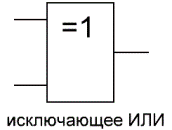
Logical element "exclusive OR".
It is customary to include an element that implements the “exclusive OR” function among the basic logical elements. Otherwise, this function is called “unequivalence”.
A high output potential occurs only if the input signals are unequal. That is, one of the inputs must have a one, and the other must have a zero. If there is an inverter at the output of the logical element, then the opposite function is performed - “equivalence”. A high output potential will appear when the signals at both inputs are the same.
Truth table.
| Input X1 | Input X2 | Output Y |
|---|---|---|
| 0 | 0 | 0 |
| 1 | 0 | 1 |
| 0 | 1 | 1 |
| 1 | 1 | 0 |
These logic elements find their application in adders. "Exclusive OR" is depicted in diagrams with an equal sign before the unit " =1 ".

In foreign style, “exclusive OR” is called XOR and on the diagrams they draw it like this.

In addition to the above logical elements, which perform basic logical functions very often, elements combined in various combinations are used. For example, K555LR4. It is called very seriously 2-4AND-2OR-NOT.

Its truth table is not given, since the microcircuit is not a basic logical element. Such microcircuits perform special functions and are much more complex than the example given. The logical basis also includes simple elements “AND” and “OR”. But they are used much less frequently. One may wonder why this logic is called transistor-transistor logic.
If you look in the reference literature for a diagram of, say, element 2I - NOT from the K155LA3 microcircuit, then you can see several transistors and resistors there. In fact, there are no resistors or diodes in these microcircuits. Only transistors are sprayed onto the silicon crystal through a stencil, and the functions of resistors and diodes are performed by the emitter junctions of the transistors. In addition, multi-emitter transistors are widely used in TTL logic. For example, at the input of element 4I there is a four-emitter
An electrical circuit designed to perform some logical operation on input data is called a logic element. The input data is represented here in the form of voltages of various levels, and the result of the logical operation at the output is also obtained in the form of a voltage of a certain level.
In this case, the operands are supplied - signals in the form of a high or low level voltage are received at the input of the logic element, which essentially serve as input data. Thus, a high level voltage - a logical 1 - indicates a true value of the operand, and a low level voltage 0 - a false value. 1 - TRUE, 0 - FALSE.
Logic element- an element that implements certain logical relationships between input and output signals. Logic gates are commonly used to construct logic circuits computers, discrete automatic monitoring and control circuits. All types of logical elements, regardless of their physical nature, are characterized by discrete values of input and output signals.
Logic elements have one or more inputs and one or two (usually inverse to each other) outputs. The values of “zeros” and “ones” of the output signals of logical elements are determined by the logical function that the element performs, and the values of “zeros” and “ones” of the input signals, which play the role of independent variables. There are elementary logical functions from which any complex logical function can be composed.
Depending on the design of the element circuit, on its electrical parameters, The logic levels (high and low voltage levels) of the input and output have the same values for the high and low (true and false) states.

Traditionally, logic elements are produced in the form of special radio components - integrated circuits. Logical operations such as conjunction, disjunction, negation and modulo addition (AND, OR, NOT, XOR) are the basic operations performed on the main types of logical gates. Next, let's look at each of these types of logic elements more closely.
Logic element "AND" - conjunction, logical multiplication, AND

“AND” is a logical element that performs a conjunction or logical multiplication operation on the input data. This element can have from 2 to 8 (the most common in production are “AND” elements with 2, 3, 4 and 8 inputs) inputs and one output.
Symbols of logical elements “AND” with different numbers of inputs are shown in the figure. In the text, a logical element “AND” with a certain number of inputs is designated as “2I”, “4I”, etc. - an “AND” element with two inputs, with four inputs, etc.

The truth table for element 2I shows that the output of the element will be a logical one only if logical ones are simultaneously at the first input AND at the second input. In the remaining three possible cases, the output will be zero.
In Western diagrams, the I element icon has a straight line at the input and a rounded line at the output. On domestic diagrams - a rectangle with the symbol “&”.
Logical element "OR" - disjunction, logical addition, OR
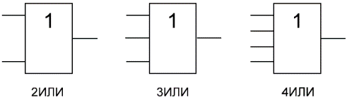
“OR” is a logical element that performs a disjunction or logical addition operation on the input data. It, like the “I” element, is available with two, three, four, etc. inputs and one output. The symbols of logical elements "OR" with different numbers of inputs are shown in the figure. These elements are designated as follows: 2OR, 3OR, 4OR, etc.

The truth table for the “2OR” element shows that for a logical one to appear at the output, it is sufficient that the logical one be at the first input OR at the second input. If there are logical ones at two inputs at once, the output will also be one.
In Western diagrams, the “OR” element icon has a rounded input and a rounded, pointed output. On domestic diagrams there is a rectangle with the symbol “1”.
Logic element "NOT" - negation, inverter, NOT
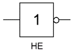
“NOT” is a logical element that performs a logical negation operation on the input data. This element, which has one output and only one input, is also called an inverter, since it actually inverts (reverses) the input signal. The figure shows the symbol for the logical element “NOT”.

The truth table for an inverter shows that a high input potential produces a low output potential and vice versa.
In Western diagrams, the “NOT” element icon has the shape of a triangle with a circle at the output. On domestic diagrams there is a rectangle with the symbol “1”, with a circle at the output.
Logic element "NAND" - conjunction (logical multiplication) with negation, NAND
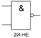
“AND-NOT” is a logical element that performs a logical addition operation on the input data, and then a logical negation operation, the result is sent to the output. In other words, it is basically an “AND” element, complemented by a “NOT” element. The figure shows the symbol for the logical element “2AND-NOT”.

The truth table for the NAND gate is the opposite of the truth table for the AND gate. Instead of three zeros and a one, there are three ones and a zero. The NAND element is also called the “Schaeffer element” in honor of the mathematician Henry Maurice Schaeffer, who first noted its significance in 1913. Denoted as “I”, only with a circle at the output.
Logical element "OR-NOT" - disjunction (logical addition) with negation, NOR
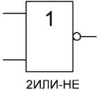
“OR-NOT” is a logical element that performs a logical addition operation on the input data, and then a logical negation operation, the result is sent to the output. In other words, this is an “OR” element supplemented by a “NOT” element - an inverter. The figure shows the symbol for the logical element “2OR-NOT”.

The truth table for an OR gate is the opposite of the truth table for an OR gate. A high output potential is obtained only in one case - low potentials are simultaneously applied to both inputs. It is designated as “OR”, only with a circle at the output indicating inversion.
Logic gate "exclusive OR" - addition modulo 2, XOR
“exclusive OR” is a logical element that performs a logical addition operation modulo 2 on the input data, has two inputs and one output. Often these elements are used in control circuits. The figure shows the symbol for this element.
The image in Western circuits is like “OR” with an additional curved strip on the input side, in domestic ones it is like “OR”, only instead of “1” it will be written “=1”.

This logical element is also called “unequivalence”. A high voltage level will be at the output only when the signals at the input are not equal (one is one, the other is zero, or one is zero, and the other is one), even if there are two ones at the input at the same time, the output will be zero - this is the difference from "OR". These logic elements are widely used in adders.
Behavior
The Exclusive OR, Exclusive NOR, Odd and Even elements calculate the corresponding function of the input values and output the result.
By default, unconnected inputs are ignored - that is, unless the inputs actually have anything connected to them - not even wires. So you can add a 5-input element, but only connect two inputs, and it will act as a 2-input element; this saves you from having to worry about setting the number of inputs every time you create an element. (If all inputs are not connected, then the error value at the output is X.) Some users, however, prefer that Logisim insist that all inputs be connected, as this matches the real elements. You can enable this behavior by selecting Project > Options..., going to the Modeling tab, and selecting the Error for Undefined Inputs option for Element Output on Uncertainty.
The two-input truth table for the elements is as follows.
| x | y | Exclusive OR | Exclusive OR NOT | Odd parity | Parity |
|---|---|---|---|---|---|
| 0 | 0 | 0 | 1 | 0 | 1 |
| 0 | 1 | 1 | 0 | 1 | 0 |
| 1 | 0 | 1 | 0 | 1 | 0 |
| 1 | 1 | 0 | 1 | 0 | 1 |
As you can see, the Odd and XOR gates behave the same in the case of two inputs; similarly, the Parity and Exclusive NOR elements behave the same. But if there are more than two inputs with a certain value, then the Exclusive OR element will output 1 when one is exactly one input, while the Odd element will output 1 when there is one on an odd number of inputs. The XOR gate will produce 1 at the output when inputs with one are strictly Not one, while the Parity element will give 1 when there are an even number of inputs with one. The XOR and XNOR gates have an attribute called Multi-Input Behavior that allows them to be configured to use the behavior of the Odd and Even gates.
If any of the inputs have an error value (for example, if conflicting values are supplied to the same wire) or a floating value, then the output will be an error value.
The multi-bit versions of each element will perform their one-bit conversions on the inputs bitwise.
Note: Many experts argue that the behavior of the XOR curly element should correspond to the behavior of the Odd element, but there is no agreement on this issue. Logisim's default behavior for the XOR element is based on the IEEE 91 standard. This is also consistent with the intuitive understanding of the term Exclusive OR: A waiter asking whether you want a side dish of mashed potatoes, carrots, green peas, or slaw will only accept one choice, not three, no matter what some experts may tell you. (I must admit, however, that I have not seriously tested this statement.) You can configure the XOR and XNOR gates to use one of the variants by changing its Multi-Input Behavior attribute.
Contacts (assuming the component is facing east)
West edge (inputs, bit width corresponds to the Data Bits attribute)Component inputs. There will be as many of them as indicated in the Number of inputs attribute.
Note that if you use curly elements, the western edge of the XOR and XNOR elements will be curved. However, the input pins are hardly located. Logisim draws short segments to show this; if you overlap a segment, the program will assume without warning that you did not mean to overlap it. When using "Print View", these segments will not be drawn if they are not connected to wires.
East edge (output, bit width corresponds to the Data Bits attribute)
The output of an element whose value is calculated based on the current values at the inputs, as described above.
Attributes
When a component is selected, or has already been added, the 0 to 9 keys change its Number of Inputs attribute, Alt-0 to Alt-9 changes its Data Bits attribute, and the arrow keys change its Direction attribute.
Direction The direction of the component (its output relative to its inputs). Data Bits The width of the component's inputs and outputs. Element Size Determines whether a wide or narrow version of the component should be rendered. This does not affect the number of inputs, which is determined by the Number of Inputs attribute; however, if the number of inputs exceeds 3 (for a narrow component) or 5 (for a wide one), then the element will be rendered with "wings" to accommodate the requested number of inputs. Number of Inputs Determines how many pins on the west edge the component will have. Multi-input behavior (XOR and XNOR only) When there are three or more inputs, the output of the XOR and XNOR gates will be based on either the fact that 1 is strictly one input (the default) or on an odd number of inputs.
A bit is the minimum unit of measurement for the amount of information, since it stores one of two values - 0 (False) or 1 (True). False and True are translated into Russian as lie and truth, respectively. That is, one bit cell can be in only one state out of two possible at a time. Let me remind you that the two possible states of a bit cell are 1 and 0.
There are certain operations for manipulating bits. These operations are called logical or Boolean operations, named after one of the mathematicians, George Boole (1815-1864), who contributed to the development of this field of science.
All of these operations can be applied to any bit, regardless of whether it has a value of 0 (zero) or 1 (one). Below are the basic logical operations and examples of their use.
Logical AND operation
AND Notation: &
The logical AND operation is performed on two bits, let's call them a and b. The result of performing the logical operation AND will be equal to 1 if a and b are equal to 1, and in all other cases, the result will be equal to 0. We look at the truth table of the logical operation and.
| a(bit 1) | b(bit 2) | a(bit 1) & b(bit 2) |
|---|---|---|
| 0 | 0 | 0 |
| 0 | 1 | 0 |
| 1 | 0 | 0 |
| 1 | 1 | 1 |
Logical OR operation
OR designation: |
The logical OR operation is performed on two bits (a and b). The result of a logical OR operation will be 0 if a and b are equal to 0 (zero), and in all other (other) cases, the result will be 1 (one). We look at the truth table of the logical operation OR.
| a(bit 1) | b(bit 2) | a(bit 1) | b(bit 2) |
|---|---|---|
| 0 | 0 | 0 |
| 0 | 1 | 1 |
| 1 | 0 | 1 |
| 1 | 1 | 1 |
Logical operation exclusive OR (XOR).
XOR notation: ^
The logical exclusive OR operation is performed on two bits (a and b). The result of a logical XOR operation will be 1 (one) if one of the bits a or b is 1 (one), otherwise the result will be 0 (zero). We look at the truth table of the logical operation exclusive OR.
| a(bit 1) | b(bit 2) | a(bit 1) ^ b(bit 2) |
|---|---|---|
| 0 | 0 | 0 |
| 0 | 1 | 1 |
| 1 | 0 | 1 |
| 1 | 1 | 0 |
Logical operation NOT (not)
Notation NOT: ~
A logical operation is NOT performed on one bit. The result of this logical operation directly depends on the state of the bit. If the bit was in the zero state, then the result of NOT will be equal to one and vice versa. We look at the truth table of the logical operation NOT.
| a(bit 1) | ~a(negation of bit) |
|---|---|
| 0 | 1 |
| 1 | 0 |
Remember these 4 logical operations. Using these logical operations we can get any possible result. Read in detail about the use of logical operations in C++.
Exclusive OR elements (in English - Exclusive-OR) could also be classified as the simplest elements, but the function they perform is somewhat more complex than in the case of the AND element or the OR element. All inputs of the XOR gates are equal, but no input can block the other inputs by setting the output to one or zero.
Rice. 4.1. Designations of elements Exclusive OR: foreign (left) and domestic (right)
The Exclusive OR function means the following: a one appears at the output when only one input has a one. If there are two or more ones at the inputs, or if all inputs are zeros, then the output will be zero. The truth table of the two-input exclusive OR element is given in table. 4.1. The designations adopted in domestic and foreign schemes are shown in Fig. 4.1. The inscription on the domestic designation of the element Exclusive OR "=1" just means that the situation is highlighted when there is one and only one unit at the inputs.
There are few XOR elements in standard series. Domestic series offer LP5 microcircuits (four two-input elements with a 2C output), LL3 and LP12, which differ from LP5 in the OK output. Too specific a function is implemented by these elements.
From a mathematical point of view, the XOR element performs the operation of the so-called modulo-2 summation. Therefore, these elements are also called modulo-two adders. As noted in the previous lecture, summation modulo 2 is indicated by a plus sign enclosed in a circle.
The main use of XOR gates, directly derived from the truth table, is to compare two input signals. In the case when two ones or two zeros arrive at the inputs (the signals coincide), a zero is formed at the output (see Table 4.1). Typically, in this application, a constant level is applied to one input of the element, with which a time-varying signal arriving at the other input is compared. But much more often, special code comparator microcircuits are used to compare signals and codes, which will be discussed in the next lecture.
As a modulo 2 adder, the XOR element is also used in parallel and serial modulo 2 dividers used to calculate cyclic checksums. But these schemes will be discussed in detail in lectures 14,15.
An important application of XOR elements is a controlled inverter (Fig. 4.2). In this case, one of the element inputs is used as a control one, and an information signal is received at the other element input. If the control input is one, then the input signal is inverted, but if it is zero, it is not inverted. Most often the control signal is given constant level, determining the operating mode of the element, and the information signal is pulsed. That is, the XOR gate may or may not change the polarity of the input signal or edge, depending on the control signal.

Rice. 4.2. Exclusive OR element as a controlled inverter
In the case where there are two signals of the same polarity (positive or negative), and their simultaneous arrival is excluded, the XOR element can be used to mix these signals (Fig. 4.3). For any polarity of input signals, the output signals of the element will be positive. For positive input signals, the XOR gate will act as a 2OR gate, and for negative inputs, it will replace the 2AND-NOT gate. Such replacements can be useful in cases where some Exclusive OR elements remain unused in the circuit. However, it must be taken into account that the signal propagation delay in the XOR element is usually slightly larger (about 1.5 times) than the delay in the simplest AND, NAND, OR, NOR elements.

Rice. 4.3. Using an XOR element to mix two non-simultaneous signals

Rice. 4.4. Selecting edges of the input signal using the XOR element
Another important application of the Exclusive OR element is the formation of short pulses along any edge of the input signal (Fig. 4.4). In this case, it does not matter whether the edge of the input signal is positive or negative, a positive pulse is still generated at the output. The input signal is delayed using a capacitor or a chain of elements, and then the original signal and its delayed copy are fed to the inputs of the Exclusive OR element. In both circuits, two-input XOR elements are also used as delay elements in a non-inverting connection (zero is applied to the unused input). As a result of this conversion, we can talk about doubling the frequency of the input signal, since the output pulses follow twice as often as the input ones.
